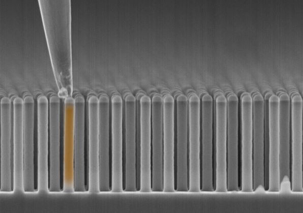
The three approaches, monolithic, transfer and Aerotaxy
Since the beginning of the project in May 2015 the members of the project have jointly pushed forward the research and development of the three approaches to nanowire synthesis and solar cell fabrication. The work is divided into work packages (WPs) which run in parallel and in the following a summary structured according to the sequence of work packages is given. We have structured our research during the two first years into three areas, involving different methods for the nanowire fabrication: a) Direct growth of III-V nanowire arrays on (100) silicon, b) Growth of nanowires of InP or GaAs, embedding these in polymer + transfer to silicon, and c) Aerotaxy growth of nanowires, alignment and array formation, embedding in polymer and transfer to silicon. These three thrusts are key for us to be able to make evaluations and decisions after the first 24 months for which approaches to give priority.

Concept I: Direct growth of nanowires on a silicon solar cell
In this approach, we use a catalyst-free growth technique to directly integrate III–V semiconducting nanowires on Si using selective area epitaxy within nanotube templates. The benefit of this template-assisted selective epitaxy (TASE) growth mode is the ability to precisely control the crystal morphology and location of the III–V nanowires, as well as to directly grow III–V materials on many Si crystalline orientations. In particular, TASE enables the growth of vertical nanowires on (001) oriented Si, which is the standard orientation used in silicon photovoltaics. Furthermore, TASE offers an attractive way to establish epitaxial contact with Si at the nanowire/Si interface, where a tunnel junction can be formed. The use of metal organic vapor phase epitaxy (MOVPE), which is a mature technique, and direct growth on Si, nano-structured by holographic methods or nano-imprint lithography, allows for large area deposition.
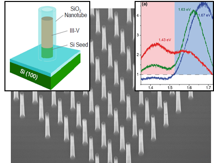
Direct growth approach (template assisted)
Concept II: Nanowire synthesized on III-V substrates for peel-off, transfer, and substrate reuse
The nanowire growth on a native III-V substrate is the most controlled process yielding high quality nanomaterials. To integrate the nanowires on a Si cell, the nanowires in concept II are transferred from their growth substrate into a membrane, which is bonded to the Si cell. The transfer can be achieved by embedding the nanowires into a polymer film and by peeling off the composite membrane. Then, the expensive III–V substrate can be reused for further growth runs.
Both tandem and four terminal architectures can be explored using this concept. Indeed, it is possible either to integrate the nanowire array by forming a direct semiconductor–semiconductor contact, or to form a semi-transparent contact on the bottom side of the composite membrane. The first option leading to a series-connected subcells requires current matching. The second option allows the top and bottom cells to operate individually with a total of four terminals, which releases the current matching requirement. In Nano-Tandem the main focus of concept II was on the second option of independently operating subcells (so called mechanically stacked architecture).
Concept III: Substrate-less nanowires grown by Aerotaxy
Nano-Tandem projects pushes forward the substrate-free synthesis technique called Aerotaxy, which offers a radical reduction of the cell cost. In Aerotaxy, nanowires grow from seed particles directly in the gas phase, and the resulting nanowire aerosol can be transferred into an ink for storage and further processing. One remarkable aspect of Aerotaxy is that this continuous process results in growth rates on the order of 1 μm/s, which is 100–1000 times faster than in metal organic vapor phase epitaxy. Size-selected catalyst particles are used to improve the nanowire homogeneity. Aerotaxy needs no lithography and is inherently scalable.
Bottom cell research
We analyzed different Si emitter structures for the Si to NW tandem configuration regarding recombination, voltage potential, interconnectivity and compatibility with subsequent processing. Highly doped emitters produced by ion-implantation were identified as most the promising. They can tolerate the absence of surface passivation, are robust in further processing and allow formation of a tunnel diode at the Si to NW interface. Fraunhofer ISE developed Si bottom cell concepts suited as base for the nanowire top cell. Samples for evaluation have been sent to the partners. Furthermore, ISE implemented a rear side light trapping concept based on a diffraction grating, leading to a bottom cell current boost of 1.2 mA/cm2 for a 280 µm thick silicon absorber compared to the planar reference.
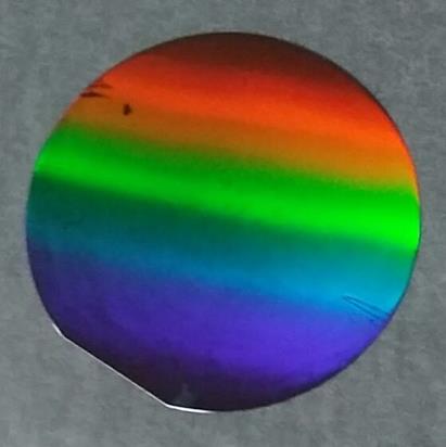
Characterization, modelling, and optimization
To successfully implement the key concept of the Nano-Tandem project, i.e. a III-V nanowire on Si tandem device, one important step is the characterization of electrical properties of nanowires integrated on Si. In particular, it is important to assess the PV generation at the scale of individual nanowires.
This challenge has been addressed using electron beam induced current (EBIC) mapping – a technique capable to localize the current generating region with very high resolution (down to 50 nm). InGaP nanowires grown on Si using template assisted selective epitaxy by IBM-Zurich were investigated. EBIC analyses revealed the current generation from an axial p-n junction within the InGaP NWs.
The profile of the generated current along the nanowire axis was used to extract material parameters, such as doping and minority carrier diffusion lengths. To improve the diffusion lengths and thus boost the conversion efficiency, a radial passivation layer is required. EBIC mapping was also applied to homogeneously doped nanowires forming a p-n junction with Si to estimate the doping level in the wires.
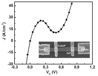
The tunnel diode is a critical component of a tandem junction solar cell. NW tunnel diodes with material combinations optimized for solar energy harvesting (typically involving ternary NW materials) have not been studied previously. We fabricated, and characterized the GaInP/InP nanowire tunnel diodes with bandgap combinations suitable for a tandem junction solar cell. Electrical measurements show that the NWs behave as tunnel diodes in both InP (bottom)/GaInP (top) and GaInP (bottom)/InP (top) configurations, exhibiting a maximum peak current density of 25 A/cm2, and maximum peak to valley current ratio of 2.5 at room temperature.
In the EBIC measurement, comparing EBIC profiles of a working and a non-working configuration confirms a wider depletion region for the non-working configuration. The realization of NW tunnel diodes in both InP/GaInP and GaInP/InP configurations lays the foundation for the next step of realizing NW tandem junction solar cells independent of the growth order of the different materials, opening up for flexibility regarding dopant incorporation polarity.
In WP 6, we have performed simulations in order to optimize the light-harvesting.
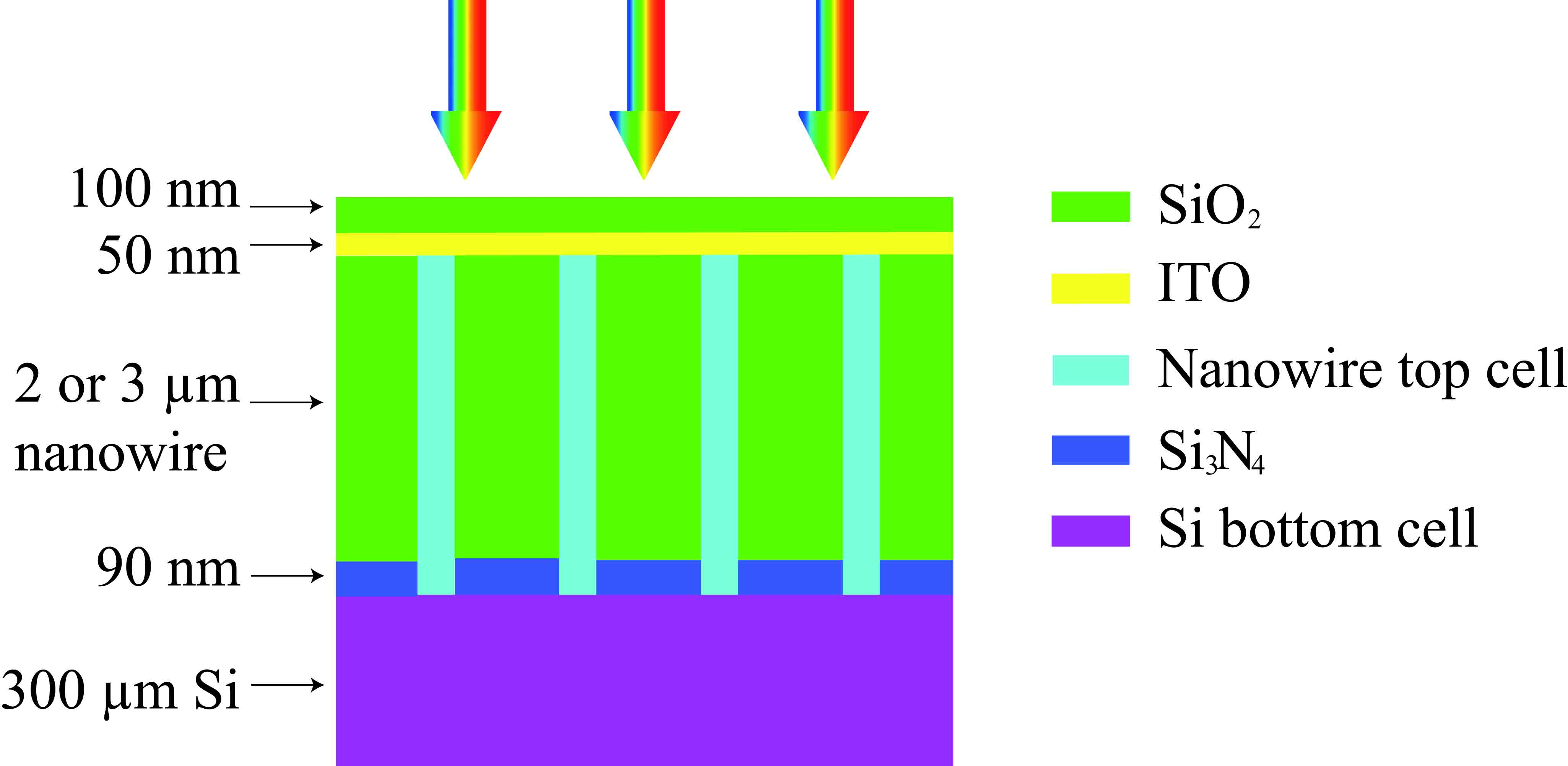
Above, a tandem solar cell design with double junctions is shown schematically. A high bandgap III-V nanowire array is used as top cell aiming to absorb the short-wavelength light. Thicker silicon solar cell is used as bottom cell aiming to absorb long-wavelength light. The geometry of top cell is optimized by maximizing the optical generated carriers in this cell and the bandgaps of top cell material are selecting by optimizing Shockley-Queisser limit. In this design, planar ITO front side contact is used instead of conformal coating to reduce the parasite absorption. To make a planar ITO, SiO2 or polymer can be used as supporting material among nanowires. Besides this ITO layer, two layers of anti-reflection coatings are used to reduce the reflection of the solar cell. A 100 nm SiO2 front side anti-reflection coating layer and a 90 nm Si3N4 at interface of silicon and nanowire can efficiently reduce the reflection from the whole structure below 4% in average.
Further reading: https://www.osapublishing.org/oe/abstract.cfm?uri=oe-25-16-A665
Life cycle assessment
We assess the environmental impact, safety and cost of the different manufacturing approaches of nanowire tandem solar cells. Preliminary life cycle assessment has showed that direct growth of nanowires on silicon substrate performs better in most impact categories – climate change, ecotoxicity, eutrophication – compared to nanowire growth on native substrate, peel-off and transfer to silicon. The reason is the additional process steps for the production of the III-V substrate and stamp fabrication.
Aerotaxy of nanowires, array formation, embedding in polymer and transfer to silicon
